PCB Designer Guide
Learn how to make mech keyboard PCBs.
- PCB Guide Part 1 - Preparations
- PCB Guide Part 2 - Beginning the project
- PCB Guide Part 3 - Creating the MCU schematic
- PCB Guide Part 4 - The rest of the schematic
- PCB Guide Part 5 - Creating the PCB
- PCB Guide Part 6 - Fill zones, decoration and production
- Example repo
- PCB Guide Part 7 - USB-C and LEDs
PCB Guide Part 1 - Preparations
Warning: This guide is outdated.
A revision is planned but yet to be created.
This guide is intended as a direct replacement for the aging Ruiqi Mao's guide.
Credits go to that guide for serving as a base for this writeup.
If you spot any mistakes, please let me know either through Discord (ai03#2725), and I will fix it to the best of my abilities.
ai03's Keyboard PCB Design Guide
So you want to design keyboard PCBs, or to make sure that you are doing things correctly.
We will build a similar 2x2 macropad in this introduction, but will do so in a more future-proof way compared to the other guides.
Step 1. Grab the requirements
We will be using KiCad for making the PCB.
Download version 5.1.4 from the previous releases folder.
Windows: https://kicad-downloads.s3.cern.ch/index.html?prefix=windows/stable/
Mac: https://kicad-downloads.s3.cern.ch/index.html?prefix=osx/stable/
Why specifically 5.1.4?
- 5.1.5 has an issue with the router which makes it extremely difficult to edit PCBs.
- 5.1.6 has an issue with part position output which can cause issues during production.
|
There are various stories about KiCad being counter-intuitive and crashing often. However, most of these stories are a relic of ancient KiCad 4.0 variants, and the program runs very stable and smooth with recent updates. However, just in case, you should always save often and use revision control (see below). |
Now comes the download and install process. Grab a cup of coffee, for the KiCad 5.1.4 installer is a whopping 1GB.
Install as you would any other program.
Also, this guide will be using Git/GitHub to manage progress.
If you are new to this, grab GitHub desktop here:
https://desktop.github.com/
Install, then sign in or create an account as necessary.
Also, make sure to become familiar with GitHub, as it is very useful for open-source projects.
| If you already work with git, use whichever implementation you prefer, and replace all mentions of GitHub in this guide with your preferred methods. |
Finally, if you would like community support in case you get stuck, I recommend that you join the Keyboard Atelier Discord server:
https://discord.gg/b7vwhHS
It is a designer haven, with references, datasheets, and various design-specific chat channels.
Step 2. Repository Preparations
First, let's create a git repository for the PCB on GitHub
It is always nice to be able to roll things back in case things get out of hand.
Also, it is a simple and reliable way of sharing your work to the world.
Select File -> New repository,
Then create a repository.
Some of the important options:
- Name - The name of the project. For now, use something like keyboard-pcb-tutorial and whatnot.
- Description - Something so that viewers won't be completely confused as to what the repository is about.
- Readme - The "front page of the repository" that's displayed when people access it on GitHub. May as well generate a blank one.
- License - Places limits on what people can do with your project. For example, you can block commercial use, force derivatives to open-source as well, etc.
This will create a blank repository to begin work in.
Publish the repository,

Using whatever settings you prefer.
Uncheck "Keep this code private" if you want to have the data public and open-source to begin with.

Repository preparations are done.
Now, it's time for initializing the KiCad project.
PCB Guide Part 2 - Beginning the project
By this point, you should have a repository readied for the project.
Step 3. Creating the KiCad project
The previous page's setup should have created a folder in your home/Documents/GitHub folder with the project name.

We will be doing all work here.
Launch KiCad, and you will be greeted with the main menu.

From the options, select New Project.

Browse to your repository directory.
Make sure to uncheck "Create a new directory for the project". Otherwise, you will have your project in a useless subdirectory.

KiCad will generate the basic project files.

The default project only has two files:
- The .sch file - Contains the schematic, or the electrical layout. This is where you will add the parts and wire them together, so KiCad knows what you're trying to accomplish.
- The .kicad_pcb file - Contains the physical layout. This is where you take the data from the schematic, and position and connect them all together for production.
The basic workflow is to create the schematic first so that the electric side is all set, then to lay it out on a physical PCB based on that.
At this point, let's commit our changes.
Give the commit a name, commit, and push the changes.
This guide will occasionally remind you to commit after large milestones; however, it is recommended to do so often. Losing work is not an enjoyable experience.


Step 4. Add local libraries
KiCad is built around libraries - A collection of footprints, and often schematic components bundled with it.
Footprints are the building blocks of PCBs - The sets of copper pads that the components attach to.
KiCad ships by default with support for common electrical components, such as resistors, capacitors, microcontrollers, etc.
It does not ship with exotic things, such as Cherry MX footprints, very specific USB connectors, etc.
Let's take care of that.
KiCad supports two library install types:
- Global - The library is added to the computer. This means you only have to install the library once.
However, this has the massive downside of requiring that the library be installed to view the project on another computer. This can be a hassle, especially if having the project checked by others - Local, or Project-Specific - The library is added only for the specific project. This means you will have to install the library each time; however, the project can be shared instantly without any worry about compatibility or missing libraries.
We will be using project-specific libraries.
First, we will need to pick which footprint libraries to use.
In this guide, I will be making use of the following repositories:
- My MX-Alps hybrid footprint library - For switches.
https://github.com/ai03-2725/MX_Alps_Hybrid.pretty - My random keyboard parts library - Mainly for the USB connector.
https://github.com/ai03-2725/random-keyboard-parts.pretty
We will be adding these to our project as Git Submodules - This allows us to pull new changes from them without having to manually download and overwrite the existing files.
Since the GitHub desktop application is fairly awful at managing submodules, we will opt for using the shell instead.

Then, run the following command:
git submodule add URL-OF-REPO
In this case, I will add the two repositories linked earlier.

The GitHub desktop GUI seems to have issues with committing submodules, so let's do it from the command line:
git add *
git commit -m "Add submodules"
git push
The commands adds the new submodules to the commit, creates a commit with the given name, and pushes it to GitHub.
After the push finishes, you can see that the library repositories are linked in your GitHub repository.

Now that the files are there, let's add them to the project.
First, open up your schematic file,

Select Preferences -> Manage Symbol Libraries,

Select the Project Specific Libraries tab, select Browse Libraries (Folder icon),
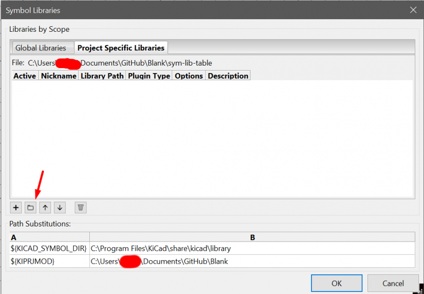
And select the .lib files in each of the added libraries.

After checking that both are added, confirm the changes by pressing OK.

Close the schematic editor for now.
Open the PCB file,

Go to Preferences -> Manage Footprint Libraries, switch to Project Specific Libraries, and browse for the added .pretty folders.
For this guide, I will be using the MX_Alps_Hybrid style footprints.

Again, click OK to confirm changes, then close the PCB editor.
Commit these changes, and push the commit.
If both the fp- and sym-lib-table files are not showing up, make sure you hit OK when adding the libraries rather than simply closing the dialog.

Now you're all prepared for making your first keyboard!
Time to begin the schematic.
PCB Guide Part 3 - Creating the MCU schematic
By this point, you should have installed the programs, created the repository, and added the local libraries.
Step 5. Beginning the schematic
The schematic is used to set up the electronics side of things.
For this tutorial, we will be using the typical Atmega32u4 microcontroller, and building a 2x2 macropad with MX and Alps support.
Open up the schematic editor to begin.

One modification used during this guide is seting the grid size to half the default size.
This allows a bit finer grain control for wiring things.
From Preferences -> Preferences -> Display options, set the grid size to 10.

Also, if you want the super HD 8K experience while making your schematic, you can swap the graphics settings in the Common page.

From Ruiqi Mao's PCB guide, here is a nice commands reference:
m: pick the component up and move it
g: drag the component up and move it while keeping wires attached to it
c: copy the component
e: edit the component
r: rotate the component
y: mirror the component
del: delete the component
esc: abort!Also, these shortcuts are useful to know:
w - Begin drawing a wire connection
k - Cut a wire and stop drawing it without clicking on an endpoint
Ctrl + h - Place a global netThe microcontroller, or MCU for short, is the brain of the PCB.
It cannot function on its own, so we will build the circuit for it.
First, press A to open the "add symbol" menu, and search for atmega32u4.
Select the atmega32u4-au component.

Place it down in the schematic.

To set it up, we will simply follow two resources:
- The technical data provided by the official datasheet.
http://ww1.microchip.com/downloads/en/devicedoc/atmel-7766-8-bit-avr-atmega16u4-32u4_datasheet.pdf - An existing "tried and tested" schematic used on the PJRC Teensy.

Usually, both a technical datasheet and an existing implementation will exist for most components.
Search for both, and use both as reference.
To begin, let's tie UVCC, VCC, and AVCC to +5V, as specified by the datasheet.
Hit P to open the power symbols menu, and select the +5V symbol.
Place it above the VCC pins. If you misplace, you can move it by hovering over the component and pressing M.

Now, wire it together using the wire tool (hotkey W).

This binds the physical UVCC/VCC/AVCC pins on the component to the +5V net.
Net refers to a set of pads that should all be connected together.
Similarly, bind the GND and UGND pins to Ground by selecting the GND symbol in the power menu and wiring them together.

Protip: It is good practice to have positive power source symbols pointing up, and ground power symbols pointing down.
Now we will place some components.
The HWB pin requires a pull-down resistor, or a resistor connected to ground.
Open the components menu with A, and search for r_small, or the small resistor component (The large one is massive and will burn space on the schematic):

Now, place this parallel to the pin labeled HWB/PE2. You can rotate the component by pressing R.
Also, place a ground symbol.

Now, wire it together.

Congratulations, now the PE2 pin is connected to ground through the resistor.
Let's change the value of the resistor. Press the E key while hovering over the resistor to edit.
A 10k ohm resistor is fit for this task. Select the value field, and type 10k.

The component's value should now be updated.

The USB pins also need resistors. Repeat the previously described commands to place two 22 ohm resistors, and wire them.

In this case, I drew the wire out on the other side as well, and used the K hotkey to end the wire at those points.
Now, let's place needed capacitors.
Through the add components menu, search for c_small (Again, regular capacitor symbol is massive).

First, place a capacitor with value 1uF beside the UCAP pin, and connect the other end to ground.

Next, we want to set up our decoupling capacitors. These are important capacitors that filter out electrical noise coming from the microcontroller.
The official documentation states to have a 0.1uF by each VCC pin (Which would be 4 on a 32u4), and a 10uF overall.
However, the Teensy schematic uses only three 0.1uF, and a 1uF overall.
I personally combine them - three 0.1uF and one 10uF. This has been confirmed functional by my testing.
Place them in an empty space close to the microcontroller, and bind one end to +5V, one end to Gnd.
Protip: Build one 0.1uF capacitor, and clone it using C to save time.

Since this PCB will get its power from USB no matter, bind VBUS to +5V.

The crystal controls how fast the controller functions.
Search for the Crystal_GND24_Small component...

...and wire the non-gnd pins (1 and 3) to XTAL1 and XTAL2.

The crystal also needs load capacitors of its own.
Place two 22pF capacitors between each crystal pin and Gnd.
Also, wire the Gnd pins on the crystal to Gnd.


Also, an external pull-up resistor can prevent the reset pin from being read faultily, and accidentally resetting during use.
For this, a 10k ohm resistor can be placed between reset and +5V.

The AREF pin is ignored since we won't be doing analog readings.
Now let's place global nets on the USB lines - These connect wires together by name, removing the need for ugly wires that cut across the entire schematic.
Hit Ctrl+H, type the names, and place them on the other end of the USB positions.

Local nets also work, but I prefer global nets since they are much more visible.

A view of the completed MCU zone.
Now, it's time to complete the rest.
PCB Guide Part 4 - The rest of the schematic
By this point, you should have the MCU schematic zone complete.
Step 6. The rest of the schematic
The rest of the schematic is not as difficult as the MCU.
Let's power through it.
USB circuitry
Only typical Mini-B USB will be covered here for simplicity reasons?
Type-C setups will be discussed in future sections.
Search for the molex USB connector in my library, along with polyfuse-small.
The polyfuse prevents your computer from exploding in case of a short circuit.
Connect VBUS -> Polyfuse, then Polyfuse -> +5V. Drop a VCC symbol pre-fuse. Change fuse value to 500mA.


The rest are self-explanatory. The data lines are connected using the global labels we set up earlier:

Switch matrix
Now, let's add the switch matrix.
I will use the MX-NoLED symbol from my own library.
Combine it with a D_Small (small diode). Ignore the LED pads for now; that will be covered later.
Connect the anode of the diode to the ROW pin of the switch.

Now clone this four times as shown:

Then, drag a wire across the diode cathode and COL pins of each row and column, and terminate them using the hotkey k:

Finally, add global labels for each row and column. It is recommended to label them counting from 0 up, since that is how it is handled firmware side as well.

Note that we will NOT be connecting the rows and columns to the MCU just yet.
Finally, a schematic is complete.
Note: The schema has pin 15 and 24 (gnd and avcc) untied. These should be tied to the GND and +5V nets respectively.

However, there's one more step before getting to work on the physical PCB.
Step 7. Assigning Footprints
As of now, the electrical setup is complete.
However, KiCad doesn't know how to translate this to physical form.
Let's input the data.
First, click the "Assign PCB footprints to schematic" option, or CvPcb.

It will ask you to annotate the schematic. This is because we left our component names un-numbered, i.e. "R?" rather than "R1, R2, R3..." etc.
For larger boards, you will want to at least manually name each switch.
But for something of this size, let's let KiCad do the tedious work for us.
Simply hit annotate, and KiCad will number each component, then launch CvPcb.

One note is that this takes a very, very long time to start up, especially on a slow internet connection.


The left side is a list of component libraries.
The center is the list of components in the schematic.
The right is a list of component in the library selected in the left.
Components come in all shapes and sizes; however, we will use typical and common sizes suited for keyboards.
For the capacitors, we will use the 0805 footprint.
On the left side, select the Capacitor_SMD library.
Select all the capacitors...

Then double click the 0805 footprint in the right panel to assign the C_0805_2012Metric footprint to all capacitors.

Likewise, assign:
| Library | Footprint | Component |
| Diode_SMD | D_SOD-123 | All diodes |
| Resistor_SMD | R_0805_2012Metric | All resistors |
| Fuse | Fuse_1206_3216Metric | Polyfuse |
| MX_Alps_Hybrid | MX-NoLED | All MX switches |
| Crystal | Crystal_SMD_3225-4pin_3.2x2.5mm | Crystal |
| random-keyboard-parts | SKQG-1155865 | Reset switch |
| random-keyboard-parts | Molex-0548190589-Assembly | USB connector |
| Packages-QFP | TQFP-44_10x10mm_Pitch0.8mm | Atmega32u4 |
Note: Due to KiCad often renaming footprints and libraries, the names may not match up letter for letter.
Even the 32u4 has to be assigned, even though it has a footprint by default.
Press apply, save schematic, and continue once done, then close the dialog.

The schematic and footprint bindings are now ready for importing to the physical PCB layout.
Commit the changes to GitHub just in case. Time to build the PCB!
PCB Guide Part 5 - Creating the PCB
Now that the schematic is finished and footprint data has been exported, we can begin with the PCB.
Step 8. Preparing the PCB
From the KiCad menu, open the PCB file.

First, let's adjust the grid so it's fine tuned for making keyboards.
On the left pane, switch the units to mm.

Open the grid settings menu via this dropdown menu on the top toolbar:

Set the custom grid size to 0.79375mm (19.05/24). This value is just fine enough for placing diodes, and just rough enough for easily placing switches.
Set the fast switching values to custom and 5mil.
This allows fast grid switching by holding Alt+1 and Alt+2.
5mil is a value well suited for routing.

Test grid switching by holding the key combinations Alt+1 and Alt+2 in PCB editor. You will see the grid switch.
Also, this is a nice chance to tune the graphics settings to your liking, since you will be staring at this screen for a while.
In Preferences -> Preferences -> Common, adjust the graphics settings to something that looks nice, but won't blow up the GPU.

In addition, in Display Options, you can change how the grid is displayed.
I suggest using lines rather than dots, for it is much easier to view the grid this way.

Setup is complete; time to import data from the schematic.
Click the import PCB data icon on the top toolbar:

Then select the Update PCB button.

Doing so will barf out all the components onto the PCB.

First, let's position our switches.
Switch to Grid 1.
Click the component MX1, and hit M to move.
Protip: Press M without the cursor over the component to make sure the cursor is locked to the center of the footprint rather than to a pad of the footprint.
Protip 2: Use ctrl+f to select a component if too lazy to find it with your eyes.
Place it down on a blank place on the PCB.

Now, place the rest of the switches so the order matches the schematic, and so the outline overlaps perfectly (This should be easy with grid 1.)


Now, place D1-D4 close to their respective switches.
We will be placing all surface mount components on bottomside. To flip the components between sides, use the F hotkey. To rotate footprints, use R.
Bottom copper will be shown as green if you have not changed the stock settings.
I placed them facing downwards as shown.

Now to position the microcontroller components.
This is easier done in grid 2.
Select the 32u4, and place it to the side of the matrix somewhere.

Place the crystal close to the crystal pins on the MCU.
It should be as close to the MCU as possible, but not so close that nearby pins cannot be broken out.
For the purposes of this example, I will place it a fair distance away.
If you need to see which pins need to be connected, control-click a pad.
 ->
-> 
Place the load capacitors for the crystal as well.
Place each 0.1uF decoupling capacitor near the VCC/GND pin pairs on the MCU. I left the pins 43-44 pair for the 10uF.
Also, place the rest of the components relatively close to their pins.


Protip: If you ever want to reposition the MCU, you can drag-select all the MCU components, and move/rotate it as if it were a single object.

Before placing the USB connector, let's draw the edge cutout line.
This is the line along which the PCB will be cut out.
We will round the corners so people don't injure themselves with sharp corners.
Using grid 1, switch to the edge.cuts layer on the right pane, and select the arc tool.
Click the center of the arc, then the beginning and end points in counterclockwise order.

After drawing the arcs, draw the line segments between them.
If any of the arcs were out of place, they can be moved or redrawn.

Now, place the USB connector along the edge.
Place the USB resistors in parallel below.

Place the remaining components.

Now that the components are placed, we can begin routing.
Note: You can always adjust component positions during routing.
Step 9. Routing
First, we need to adjust some settings.
Switch to inch instead of mm on the left pane, and open the Board Setup menu. Then, open the Net Classes page.

By default, all tracks are roughly 10 mil wide.
However, it is always good practice to route power traces thicker whenever possible.
Add a new net class named power, set its track width to 15 mils. Set the track width for default to 10 mils as well.
Using the list on the bottom, assign the power class to the nets VCC, Gnd, and +5V (All the power nets).

Press OK to confirm changes.
Now, the remainder is connecting all of the pads of the same net.
Use the trace tool (Hotkey X), click one pad to begin, another pad to end.
Clicking empty spaces will create corners.

A few important points when doing so:
- You can route traces on both top and bottomside. Press V when not routing to switch between top and bottom, and press V while routing to drop a via, or a drill hole that allows you to jump between layers.
My usual choice is to generally route verticals on top, horizontals on bottom.
- Do not place vias in pads. This will cause solder to be "vacuumed out" by the via, leading to insufficient solder joints.
- USB data lines should be routed parallel.

- The crystal area should be kept isolated from other traces as much as possible.

- Make sure the central ground track does not enter the exposed mask areas of the xtal traces.
Change the track's width to 10 or 8mil to avoid such interference.
- The decoupling capacitors should be routed so that +5V feeds through the decoupling capacitors as shown:

Do not route +5V through the inside of the MCU or change this order of link, or the decoupling capacitor will have very little effect.
Here is a sample routed PCB.

After passing through the polyfuse, the +5V line passes through the 10uF capacitor, which acts as a general decoupler for the entire MCU. After passing through it, the +5V rail flips to the top of the PCB, where it draws a U to feed each VCC pin through its decoupling capacitor.
Step 10. Choosing the matrix pinout
You may notice that the switches are not connected to the MCU at all.
This is because the pins to connect the matrix to are best chosen depending on the circumstance.
For example, it is much more logical to use these pins to the right,

Compared to attempting to desperately use the pins at the top left corner.

First, take a note of the pins you want to use,

and in the schematic editor, place the net labels for the rows and cols on the pins you wish to use.

Read these changes into the PCB.

The connections should appear on the MCU.

Quickly route these as well.

Congratulations! You have built your first keyboard PCB.
If you are not satisfied with the routing, you can go to Edit -> Global Deletions and check Tracks to restart.
Practice routing as many times as possible - It takes experience, not reading a tutorial, to learn the little tricks to route cleanly and efficiently.
Once you are finished, commit to GitHub. Then, it's time to add the final touch.
PCB Guide Part 6 - Fill zones, decoration and production
Now that the routing is finished, let's tune the PCB up.
Step 11. Ground fills
You may remember the mention about how the crystal zone is sensitive.
We can protect it, along with other components, from external electrical noise through the use of ground fills.
Select create fill zones to begin.

We will draw two zones: One around the MCU, and one for the USB connector.
Then click on the first corner of the zone to surround to bring up a menu.

Select the ground net for the fill net, and high resolution for prettier edges.
Click at the corners, and double click at the last corner to end.
Then, press B to fill the zone.

The ground fill question is always an interesting one.
On one hand, it reduces EMI interference both entering and exiting the board.
However, it adds a significant amount of copper, making it more difficult to solder due to the necessity to raise temperatures further for ground-connected components.
It also makes the PCB opaque. This can be a major disadvantage if you are wishing for the translucent PCB aesthetic.
I will say two things regarding this topic:
- If doing full ground fill, make sure there is no ground current interference (i.e. Ground current from LED doesn't take a path that cuts across MCU/Crystal zone).
- If doing minimal ground fill, at least do the following:
- Around the crystal
- Under the MCU, possibly a bit around
- Below the USB connector
- Also, in this case, it is critical that the USB lines are routed properly: Not close and parallel to pulsing matrix and LED lines, crossing perpendicularly to other traces as much as possible.

Whether you choose aesthetic or function is up to you. Such is a design decision left for the designer.
My personal recommendation is to use fill around the entire MCU zone or entire board until you are used to PCB design and have a few functional prototypes.
Step 12. Decorations
Let's celebrate your first PCB by making it yours.
The following layers can be used for aesthetic designs:
- F/B.SilkS - Silkscreen print. The best choice for most decorations.
- F/B.Cu - The copper. Add stealth logos and text that aren't as obvious.
- F/B.Mask - The soldermask. If no copper exists below, you will end up with a tan color exposed (PCB material). If copper below, you will get a shiny copper artwork or text.
For example, select the text tool on the layer F.SilkS, and place a block of text on the PCB.
Then, press Alt+3 to render the PCB.

Artwork can be done using Bitmap2Component. This will be discussed in a future chapter.
Step 13. Error Check
Are you sure that you haven't made any mistakes?
Use DRC to find out.

Press "Start DRC", then wait a few moments for KiCad to find things to complain about.
If it returns empty, you're all set.

If not, you've made a mistake.
Double click the error to figure out what's wrong. (It will jump to the error point.)
Repeat until KiCad complains no more.
Step 14. Production
Let's get this board produced and in your hands.
Gerber files are the standard for PCB data. We will export this from KiCad.

Here are the generic settings I use for exporting to most factories.

Once everything is set, press Plot to generate the data.
Now click Generate Drill Files.
Stock settings should work fine here. Simply generate the files and close all dialogs.

Check your repository folder - You'll notice that there are gerber files in the directory you specified.


Add all these gerber files to a zip file.

Congratulations, you can use this file for production.
Commit a celebratory commit to GitHub so you don't lose your work when KiCad decides to have a bad hair day.
For example, you can upload the zip at JLCPCB, and it will generate a quick screenshot of the PCB data.

Step 15. Ordering parts
Let's finish the guide up by buying all the parts necessary to assemble this board.
| Component | Quantity | Package | Sample Part |
| Ceramic Capacitor, 0.1uF | 3 | 0805 | 1276-2450-1-ND |
| Ceramic Capacitor, 10uF | 1 | 0805 | 1276-6455-1-ND |
| Ceramic Capacitor, 1uF | 1 | 0805 | 1276-1066-1-ND |
| Ceramic Capacitor, 22pF | 2 | 0805 | 1276-2605-1-ND |
| Diode, Generic | 4 | SOD-123 | 1N4148WTPMSCT-ND |
| Polyfuse, 500mA hold, 1A trip | 1 | 1206 | 507-1803-1-ND |
| Resistor, 10k | 2 | 0805 | P10KDACT-ND |
| Resistor, 22 | 2 | 0805 | P22ACT-ND |
| Low Profile Tactile Switch | 1 | 5.2x5.2mm | CKN10361CT-ND |
| ATMEGA32U4 Microcontroller | 1 | 44TQFP 10x10mm | ATMEGA32U4-AU-ND |
| Molex Mini-B USB C Receptacle | 1 | Molex-0548190589 | WM3895CT-ND |
| Crystal, 16MHz | 1 | 3.2x2.5mm, 4 pad | 1253-1698-1-ND |
The guide will be expanded sooner or later to cover LEDs and such.
For now, you can refer to the advanced info.
Also, feel free to join ai03's Discord server.
It provides a safe place for all to discuss and design.
Example repo
https://github.com/ai03-2725/ai03-pcb-guide
This repository contains the latest version of the example PCB built following the guide.
PCB Guide Part 7 - USB-C and LEDs
Notice: This page is incomplete and is currently being written.
Let's spice up the project with a more versatile connector and a bit of eyecandy.
Step 16. Switching to C
Until this page is complete, see https://wiki.ai03.com/books/pcb-design/page/usb-type-c