# Routing Techniques
##### Tips for a proper, organized PCB
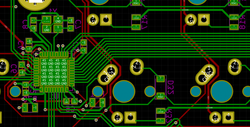
## Good Routing Techniques
- Do not route traces close to the edge.
- Do not place EMI-emitting components, such as crystals, near a board edge.
- Surround pulsating traces with proper ground plane fill to reduce EMI.
- Use front and back for horizontal and vertical traces respectively, or something similar to avoid clashing.
- Pick sides which do not force the abuse of vias for routing smd components.
- Let busses take precedence over singular traces (explained below).
- Route many traces going in the same direction together for efficient use of space.
- This can be used to efficiently break out many traces from the controller.