EMI Shielding and Reduction
Healthy PCB designing.
Important to prevent a keyboard from malfunctioning from too much outside noise, and also to prevent a keyboard from wreaking havoc upon nearby devices such as pacemakers.
Texas Instruments states that any frequency above 80 MHz is a concern for radio frequency noise, but it’s not bad to be on the safe side, especially since these tips don’t change PCB costs at all.
General Design Considerations
Surface mount v.s. Through-hole
- Surface mount often has lower noise emissions because the smaller components can be crushed together into a smaller region.
- I cannot find the source, but I have read somewhere that round plated things such as through-hole pads can act as antennas much like a via under high frequencies.
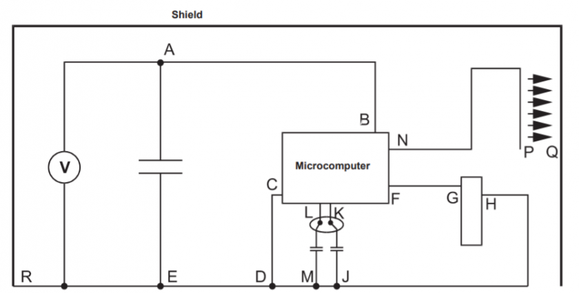
No loops - Loops are antennas.


- This diagram from the Texas Instruments guide shows two loops.
- A-B-C-D-E
- F-G-H-D-C
- Avoid them whenever possible.
Vias can act as antennas under higher frequencies. Reduce when possible.
Ground Planes
For the microprocessor:
- Extend a ground pad on the other side of the controller, at least ¼ inches out beyond the area of the controller.
- Preferably, use the ground plane to shield crucial components for the controller as well.
- Don’t use the same ground plane for the controller as the rest of the board. Noisy ground current will flow into the controller area, and will destroy the point of having a ground plane in the first place.
- Of course, this can be avoided with careful design of the ground plane.
- Simply make sure that the ground planes do not act as a road for dirty ground signal to interfere with the clean controller ground area.
- For extended shielding, place a ground plane on the other side as well.
- Again, this must follow the aforementioned rules: Do not connect the ground planes together in far distances at multiple points or it becomes a loop of its own.
- Having just one via will be effective.
- Having many vias distributed across the area at close range within each other is also effective. This will effectively turn the two planes into one huge “block” of copper.
- Preferably, separate the ground plane for the crystal from the ground plane of the controller area as well.
- Connect the controller plane to the rest of the board’s ground at only one location.
- Since electricity travels in the shortest distance possible, proper connection of the two ground planes will make the noisy ground signal from other components such as LEDs travel straight to the USB connector, disregarding the area * near the controller.
- tl;dr: Shield the controller and don’t fling dirty ground current towards the controller.
General tips and info
- A ground plane not connected to the ground (USB ground in the case of a regular keyboard) is not technically grounded.
- For a wireless keyboard, connect the ground plane to the largest ground device possible, I.E. a metal plate or metal case.
- If none of these are available, disregard this, since the ground plane itself serves as the largest ground.
- Making the ground plane go all the way to the rim of the PCB can cause some fabs to create the PCB with a bit of the ground plane visible at the edge of the PCB. This can cause short-circuiting if not careful.
- ALWAYS “rebuild” or “regenerate” the copper plane/ground plane area after changing any traces or component locations. Otherwise, the ground plane may be stuck to a bunch of other traces, causing huge short circuit issues.
- It is suggested to place the ground plane in the very end.
- This makes for easier routing.
- Even if using ground planes, route ground traces.
- This makes sure that all ground components are properly connected.
- Using ground plane brute force may end up with improper connections for sensitive components near the controller. (See section 1)
- Larger ground planes are more effective. Thin ground planes basically do nothing.
Minimal Ground Plane
For when you want maximum aesthetics.
This bare minimum setup has been tested functional:
- Ground plane around crystal, same side as crystal
- Ground plane below MCU (for TQFP)
- Ground plane below USB connector
- Carefully isolating USB data lines, making sure other lines cross at 90 degree angles
Only attempt this if you are comfortable with careful component positioning and whatnot.
Via Fencing
It’s exactly how it sounds.
- Placing multiple ground vias in a line, connected on both sides to a non-noisy ground trace/area, acts as a “fence” or “wall” to vacuum the ugliest RF noise.
- Larger vias work better (Larger wall)
Calculating distance between vias
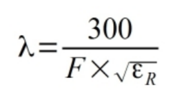
- At least 1/10 of wavelength
- At least 1/20 of wavelength recommended
- Based on this excerpt from EDN’s PDF:


- A common 16MHz signal used in keyboards has a wavelength of at least 23 inches, so the via spacing must be at most greater than 1 inches apart. Nothing to worry about here.
Preferably, more vias = greater effect, but more vias = more drilling = higher PCB cost sometimes. Don’t overdo them to prevent turnaround time from skyrocketing or extra charges from piling up.
Uses
- Can be used to reinforce sensitive areas, such as the area around the controller.
- This is an example of keeping RF interference out.
- Can be used when pulsing traces are too close to the edge of the PCB for the ground plane to effectively soak up the noise from exiting the board.
- Simply make an effective ground plane between the trace and the edge of the board.
- This is an example of keeping EMI in.
Sources
http://www.ti.com/lit/an/szza009/szza009.pdf
http://www.edn.com/Pdf/ViewPdf?contentItemId=4406491
https://electronics.stackexchange.com/questions/41871/via-fences-for-noise-reduction-of-a-chip-antenna
http://www.edn.com/Pdf/ViewPdf?contentItemId=4406491