
PCB Guide Part 4 - The rest of the schematic
By this point, you should have the MCU schematic zone complete.
Step 6. The rest of the schematic
The rest of the schematic is not as difficult as the MCU.
Let's power through it.
USB circuitry
Only typical Mini-B USB will be covered here for simplicity reasons?
Type-C setups will be discussed in future sections.
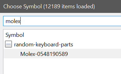
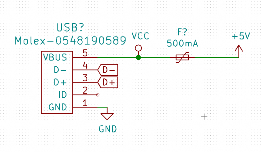
Search for the molex USB connector in my library, along with polyfuse-small.
The polyfuse prevents your computer from exploding in case of a short circuit.
Connect VBUS -> Polyfuse, then Polyfuse -> +5V. Drop a VCC symbol pre-fuse. Change fuse value to 500mA.
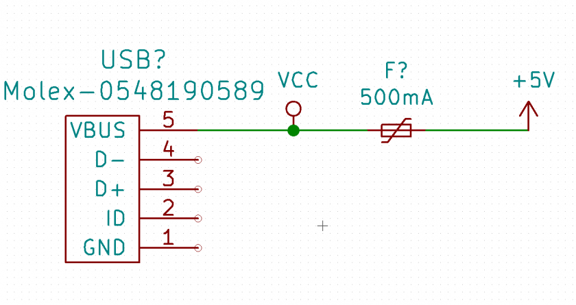
The rest are self-explanatory. The data lines are connected using the global labels we set up earlier:
Switch matrix
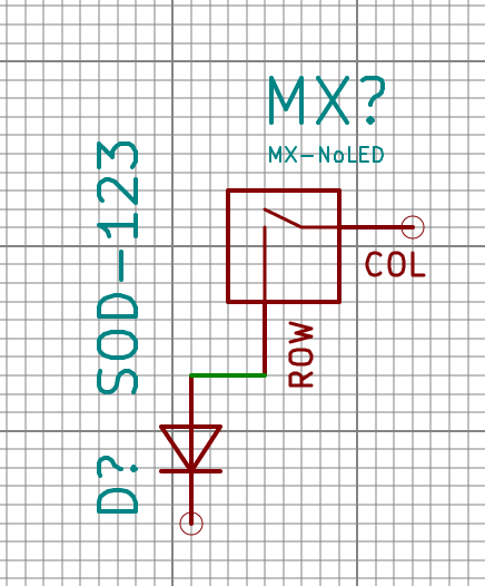
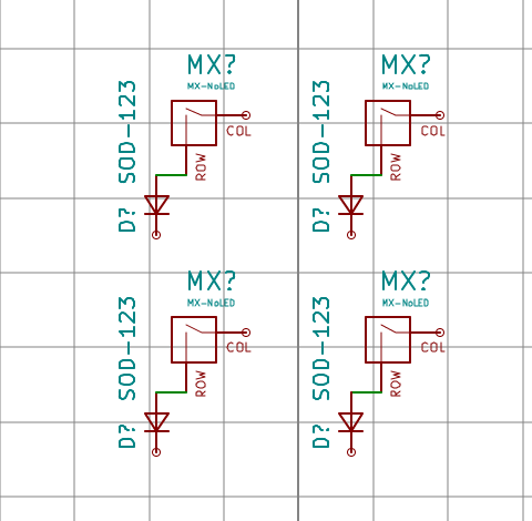
Now, let's add the switch matrix.
I will use the MX-NoLED symbol from my own library.
Combine it with a D_Small (small diode). Ignore the LED pads for now; that will be covered later.
Connect the anode of the diode to the ROW pin of the switch.
Now clone this four times as shown:
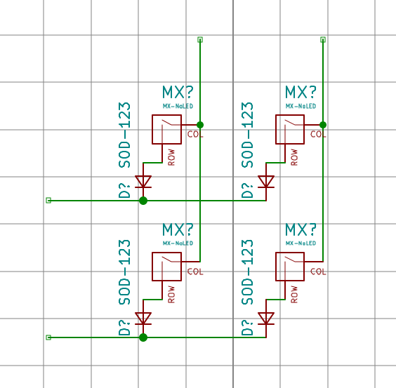
Then, drag a wire across the diode cathode and COL pins of each row and column, and terminate them using the hotkey k:
Finally, add global labels for each row and column. It is recommended to label them counting from 0 up, since that is how it is handled firmware side as well.
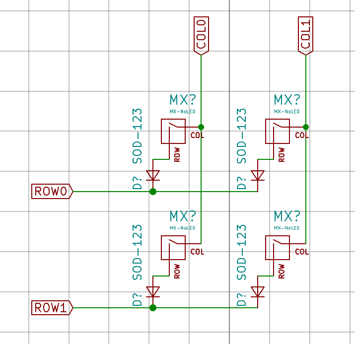
Note that we will NOT be connecting the rows and columns to the MCU just yet.
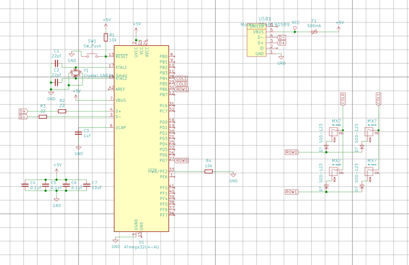
Finally, a schematic is complete.
Note: The schema has pin 15 and 24 (gnd and avcc) untied. These should be tied to the GND and +5V nets respectively.
However, there's one more step before getting to work on the physical PCB.
Step 7. Assigning Footprints
As of now, the electrical setup is complete.
However, KiCad doesn't know how to translate this to physical form.
Let's input the data.
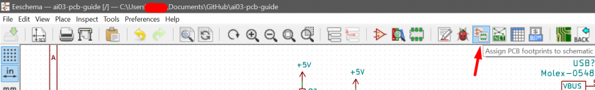
First, click the "Assign PCB footprints to schematic" option, or CvPcb.
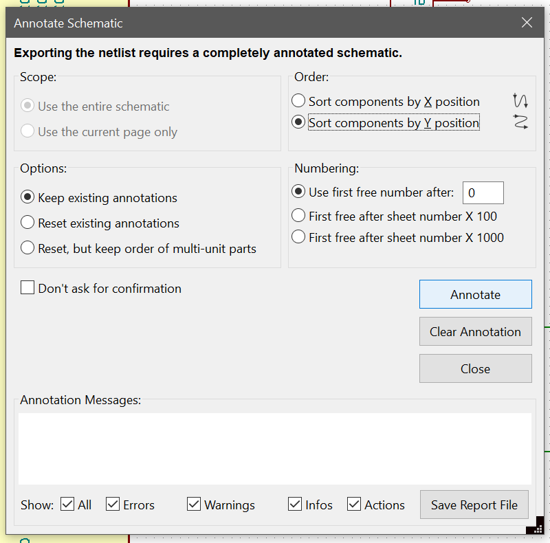
It will ask you to annotate the schematic. This is because we left our component names un-numbered, i.e. "R?" rather than "R1, R2, R3..." etc.
For larger boards, you will want to at least manually name each switch.
But for something of this size, let's let KiCad do the tedious work for us.
Simply hit annotate, and KiCad will number each component, then launch CvPcb.
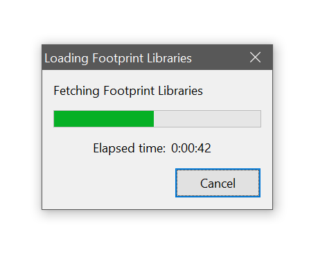
One note is that this takes a very, very long time to start up, especially on a slow internet connection.
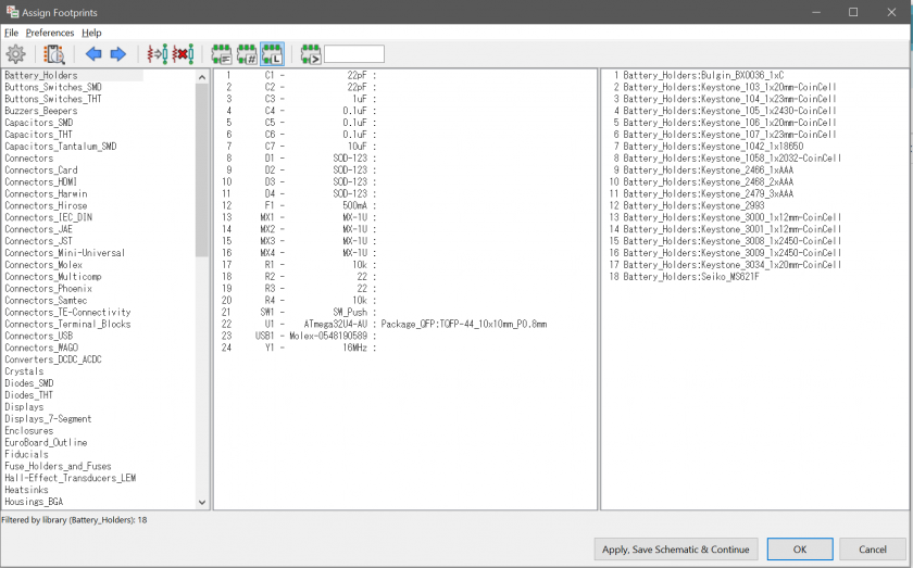
The left side is a list of component libraries.
The center is the list of components in the schematic.
The right is a list of component in the library selected in the left.
Components come in all shapes and sizes; however, we will use typical and common sizes suited for keyboards.
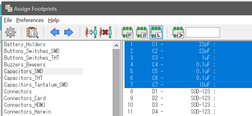
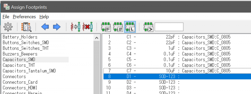
For the capacitors, we will use the 0805 footprint.
On the left side, select the Capacitor_SMD library.
Select all the capacitors...
Then double click the 0805 footprint in the right panel to assign the C_0805_2012Metric footprint to all capacitors.
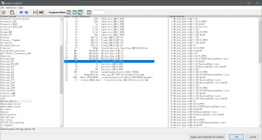
Likewise, assign:
| Library | Footprint | Component |
| Diode_SMD | D_SOD-123 | All diodes |
| Resistor_SMD | R_0805_2012Metric | All resistors |
| Fuse | Fuse_1206_3216Metric | Polyfuse |
| MX_Alps_Hybrid | MX-NoLED | All MX switches |
| Crystal | Crystal_SMD_3225-4pin_3.2x2.5mm | Crystal |
| random-keyboard-parts | SKQG-1155865 | Reset switch |
| random-keyboard-parts | Molex-0548190589-Assembly | USB connector |
| Packages-QFP | TQFP-44_10x10mm_Pitch0.8mm | Atmega32u4 |
Note: Due to KiCad often renaming footprints and libraries, the names may not match up letter for letter.
Even the 32u4 has to be assigned, even though it has a footprint by default.
Press apply, save schematic, and continue once done, then close the dialog.
The schematic and footprint bindings are now ready for importing to the physical PCB layout.
Commit the changes to GitHub just in case. Time to build the PCB!