
PCB Guide Part 5 - Creating the PCB
Now that the schematic is finished and footprint data has been exported, we can begin with the PCB.
Step 8. Preparing the PCB
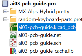
From the KiCad menu, open the PCB file.
First, let's adjust the grid so it's fine tuned for making keyboards.
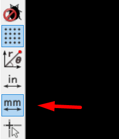
On the left pane, switch the units to mm.
Open the grid settings menu via this dropdown menu on the top toolbar:
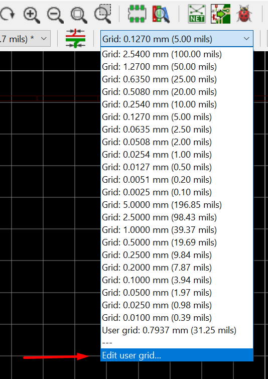
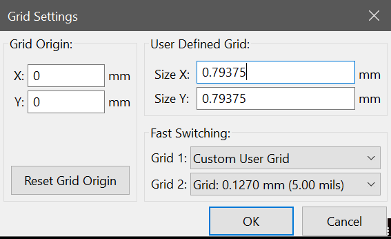
Set the custom grid size to 0.79375mm (19.05/24). This value is just fine enough for placing diodes, and just rough enough for easily placing switches.
Set the fast switching values to custom and 5mil.
This allows fast grid switching by holding Alt+1 and Alt+2.
5mil is a value well suited for routing.
Test grid switching by holding the key combinations Alt+1 and Alt+2 in PCB editor. You will see the grid switch.
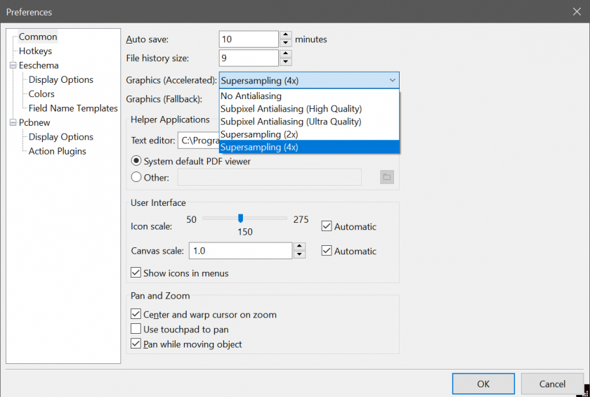
Also, this is a nice chance to tune the graphics settings to your liking, since you will be staring at this screen for a while.
In Preferences -> Preferences -> Common, adjust the graphics settings to something that looks nice, but won't blow up the GPU.
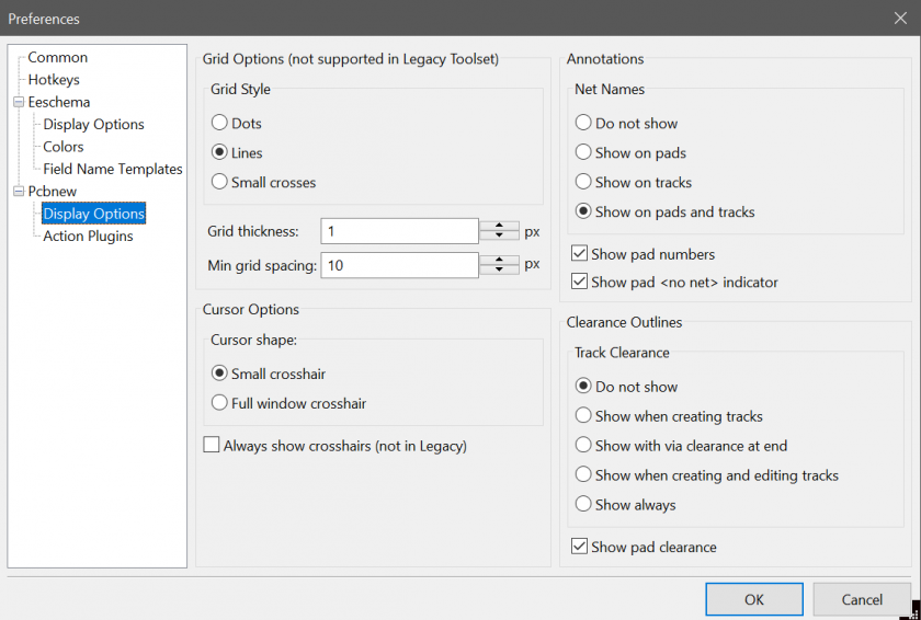
In addition, in Display Options, you can change how the grid is displayed.
I suggest using lines rather than dots, for it is much easier to view the grid this way.
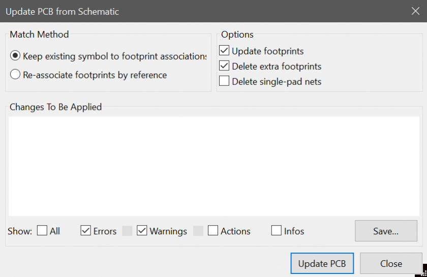
Setup is complete; time to import data from the schematic.
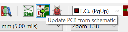
Click the import PCB data icon on the top toolbar:
Then select the Update PCB button.
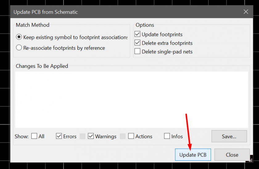
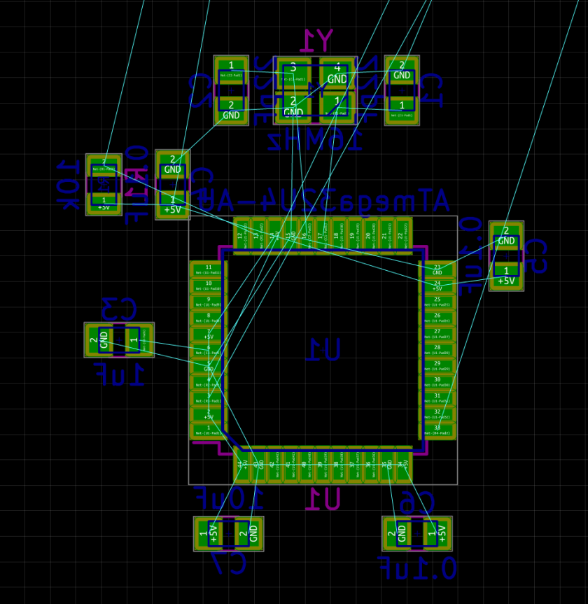
Doing so will barf out all the components onto the PCB.
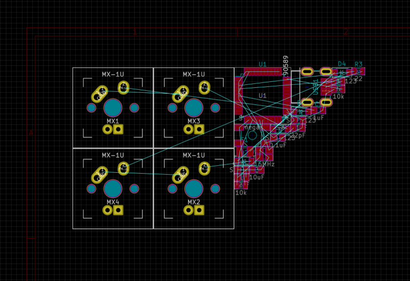
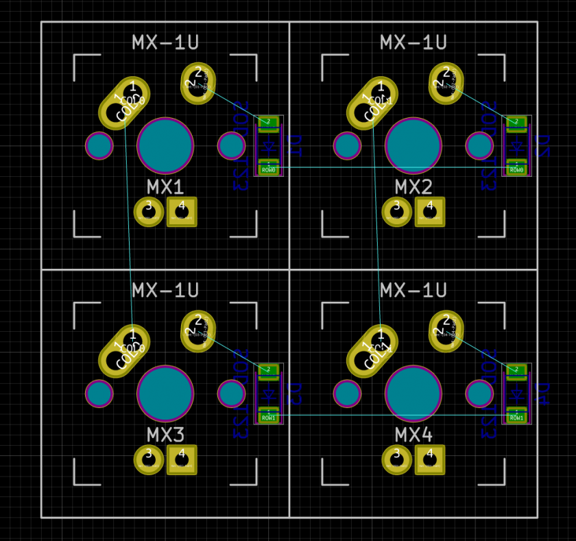
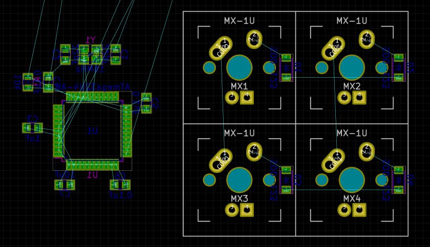
First, let's position our switches.
Switch to Grid 1.
Click the component MX1, and hit M to move.
Protip: Press M without the cursor over the component to make sure the cursor is locked to the center of the footprint rather than to a pad of the footprint.
Protip 2: Use ctrl+f to select a component if too lazy to find it with your eyes.
Place it down on a blank place on the PCB.
Now, place the rest of the switches so the order matches the schematic, and so the outline overlaps perfectly (This should be easy with grid 1.)
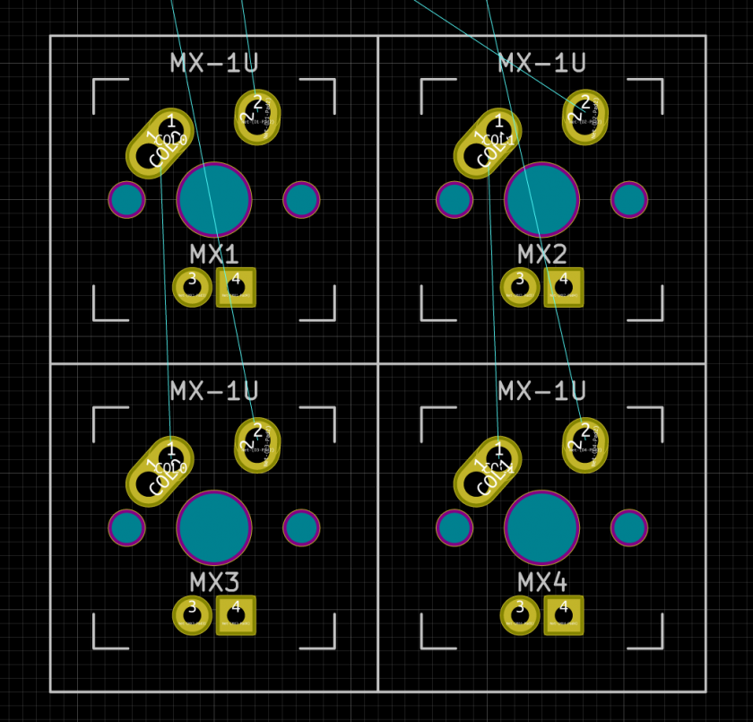
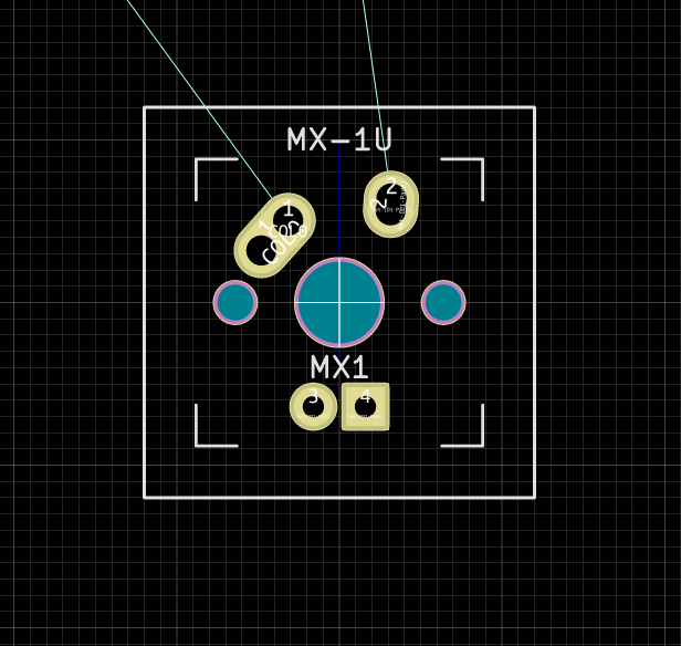
Now, place D1-D4 close to their respective switches.
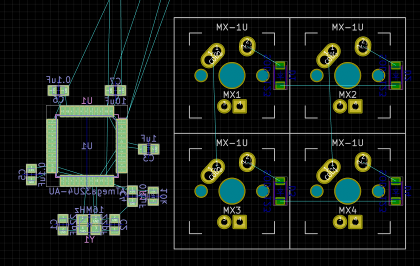
We will be placing all surface mount components on bottomside. To flip the components between sides, use the F hotkey. To rotate footprints, use R.
Bottom copper will be shown as green if you have not changed the stock settings.
I placed them facing downwards as shown.
Now to position the microcontroller components.
This is easier done in grid 2.
Select the 32u4, and place it to the side of the matrix somewhere.
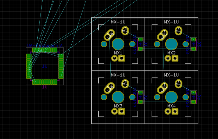
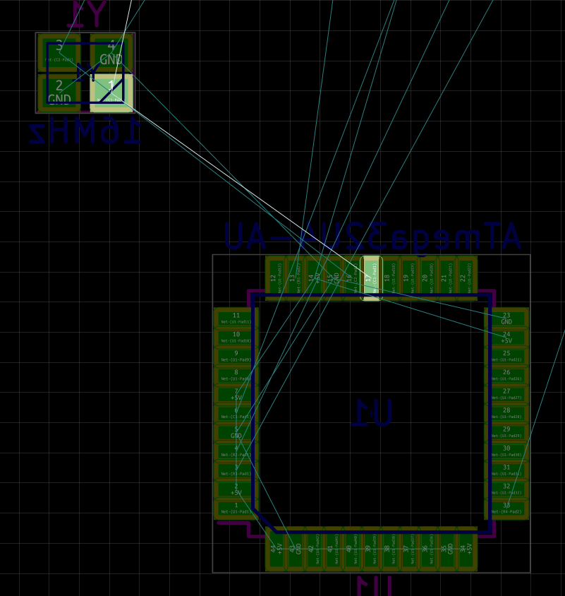
Place the crystal close to the crystal pins on the MCU.
It should be as close to the MCU as possible, but not so close that nearby pins cannot be broken out.
For the purposes of this example, I will place it a fair distance away.
If you need to see which pins need to be connected, control-click a pad.
 ->
-> 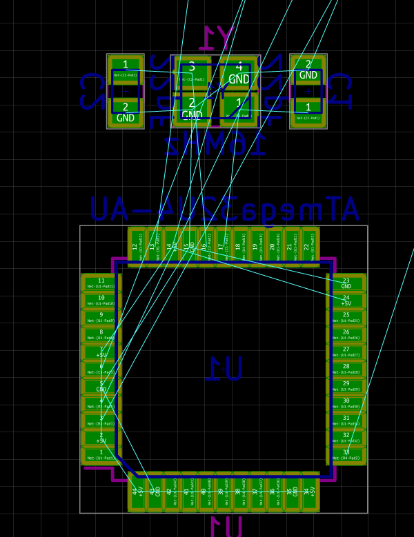
Place the load capacitors for the crystal as well.
Place each 0.1uF decoupling capacitor near the VCC/GND pin pairs on the MCU. I left the pins 43-44 pair for the 10uF.
Also, place the rest of the components relatively close to their pins.
Protip: If you ever want to reposition the MCU, you can drag-select all the MCU components, and move/rotate it as if it were a single object.
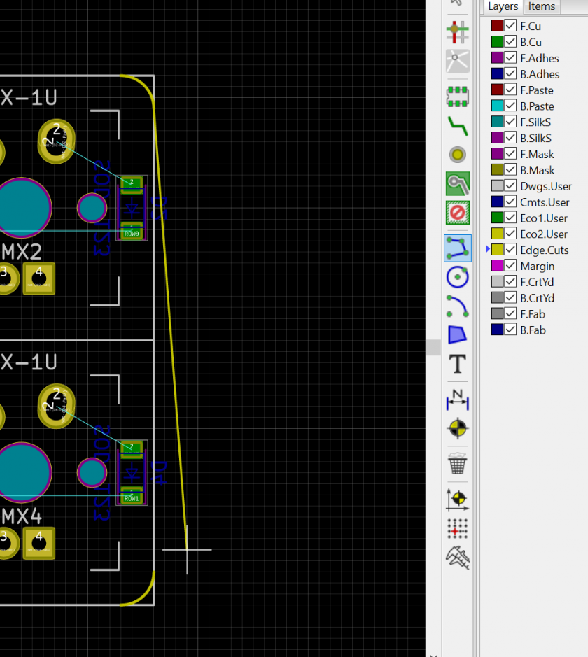
Before placing the USB connector, let's draw the edge cutout line.
This is the line along which the PCB will be cut out.
We will round the corners so people don't injure themselves with sharp corners.
Using grid 1, switch to the edge.cuts layer on the right pane, and select the arc tool.
Click the center of the arc, then the beginning and end points in counterclockwise order.
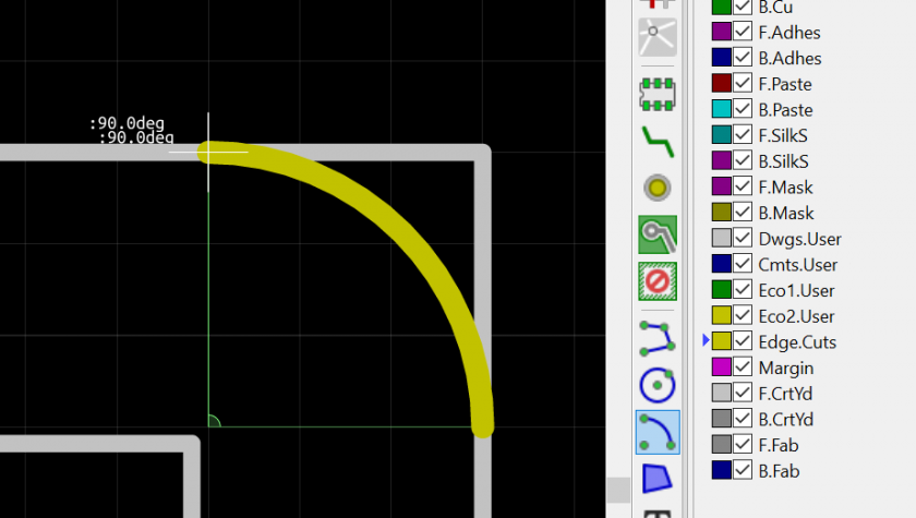
After drawing the arcs, draw the line segments between them.
If any of the arcs were out of place, they can be moved or redrawn.
Now, place the USB connector along the edge.
Place the USB resistors in parallel below.
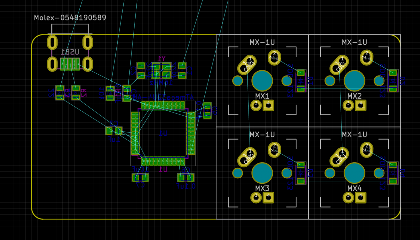
Place the remaining components.
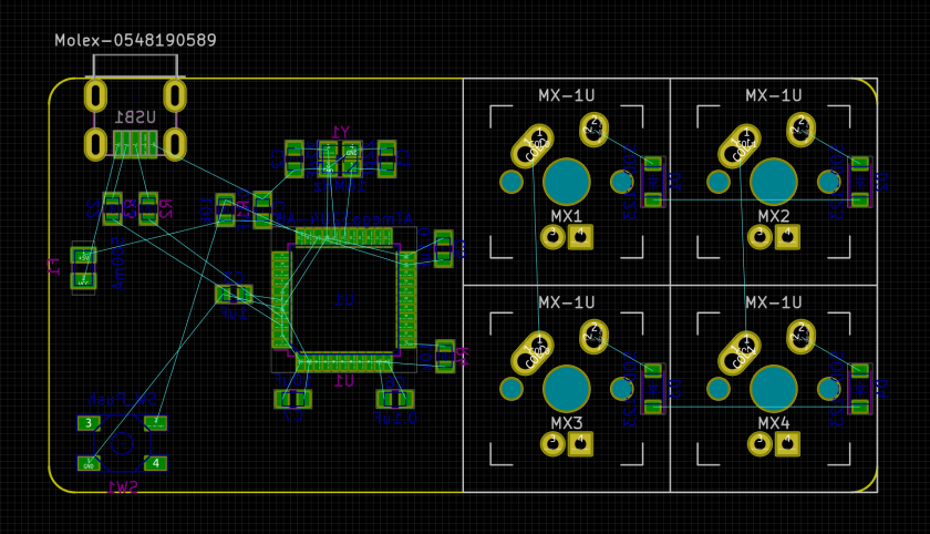
Now that the components are placed, we can begin routing.
Note: You can always adjust component positions during routing.
Step 9. Routing
First, we need to adjust some settings.
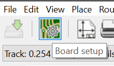
Switch to inch instead of mm on the left pane, and open the Board Setup menu. Then, open the Net Classes page.
By default, all tracks are roughly 10 mil wide.
However, it is always good practice to route power traces thicker whenever possible.
Add a new net class named power, set its track width to 15 mils. Set the track width for default to 10 mils as well.
Using the list on the bottom, assign the power class to the nets VCC, Gnd, and +5V (All the power nets).
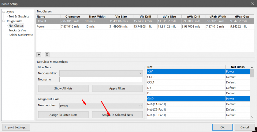
Press OK to confirm changes.
Now, the remainder is connecting all of the pads of the same net.
Use the trace tool (Hotkey X), click one pad to begin, another pad to end.
Clicking empty spaces will create corners.
A few important points when doing so:
- You can route traces on both top and bottomside. Press V when not routing to switch between top and bottom, and press V while routing to drop a via, or a drill hole that allows you to jump between layers.
My usual choice is to generally route verticals on top, horizontals on bottom.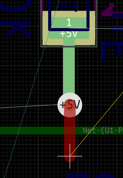
- Do not place vias in pads. This will cause solder to be "vacuumed out" by the via, leading to insufficient solder joints.
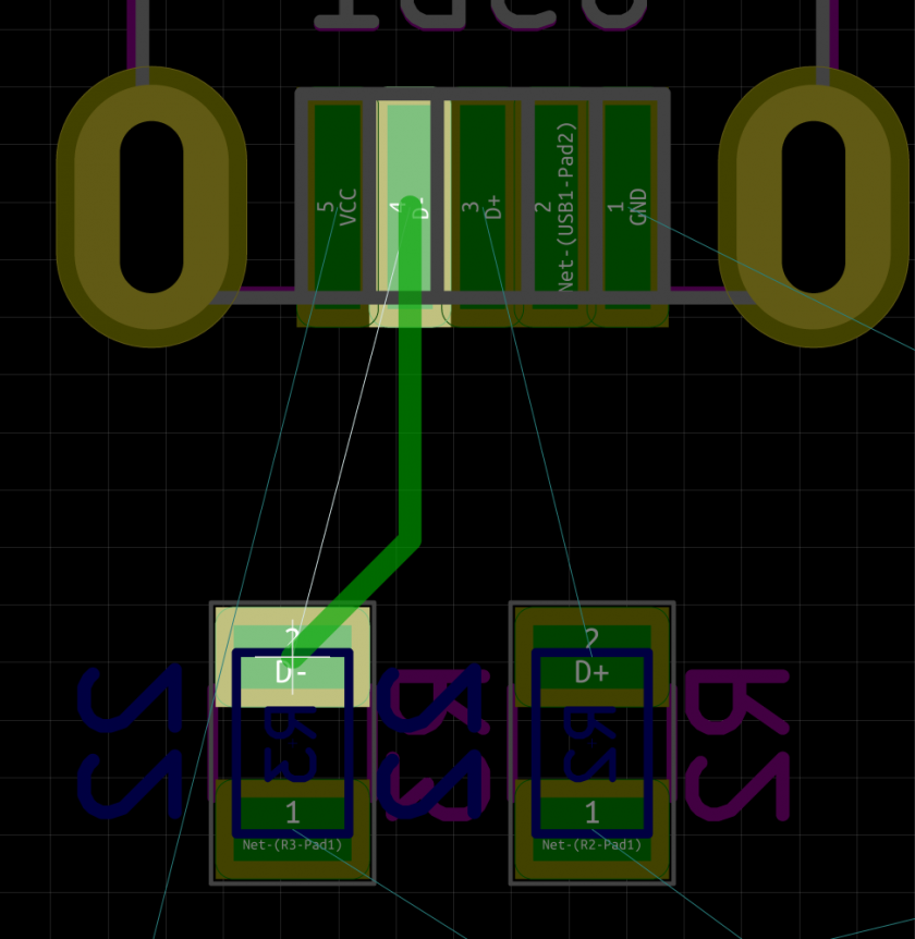
- USB data lines should be routed parallel.
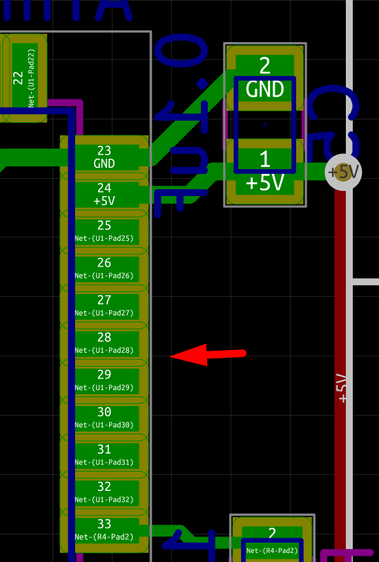
- The crystal area should be kept isolated from other traces as much as possible.
- Make sure the central ground track does not enter the exposed mask areas of the xtal traces.
Change the track's width to 10 or 8mil to avoid such interference.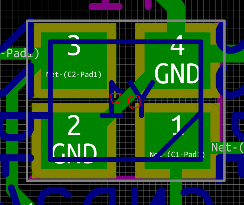
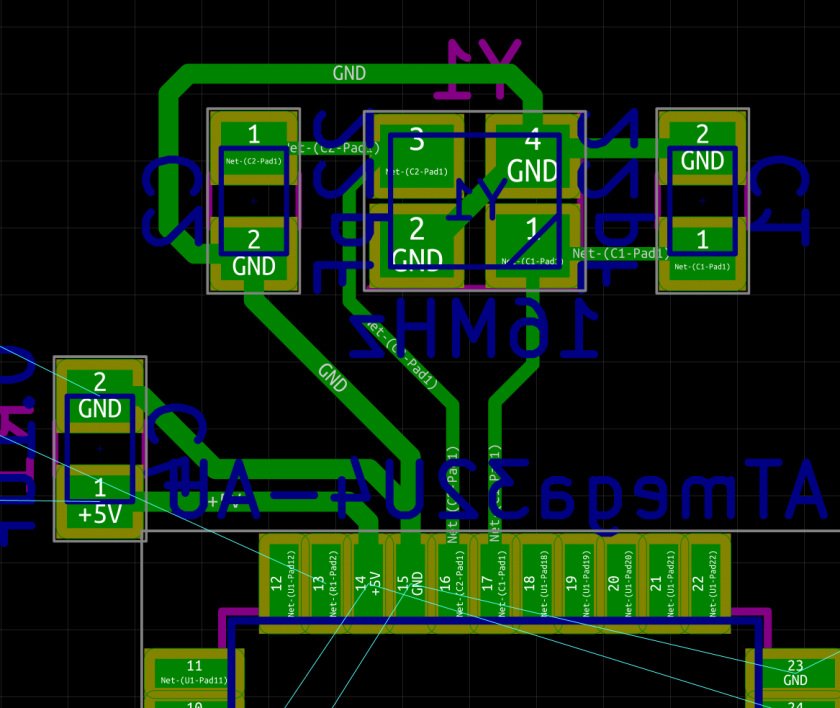
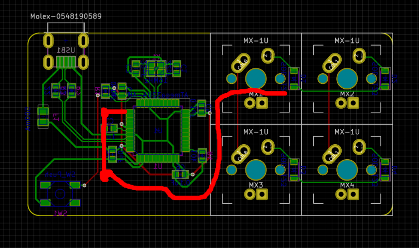
- The decoupling capacitors should be routed so that +5V feeds through the decoupling capacitors as shown:
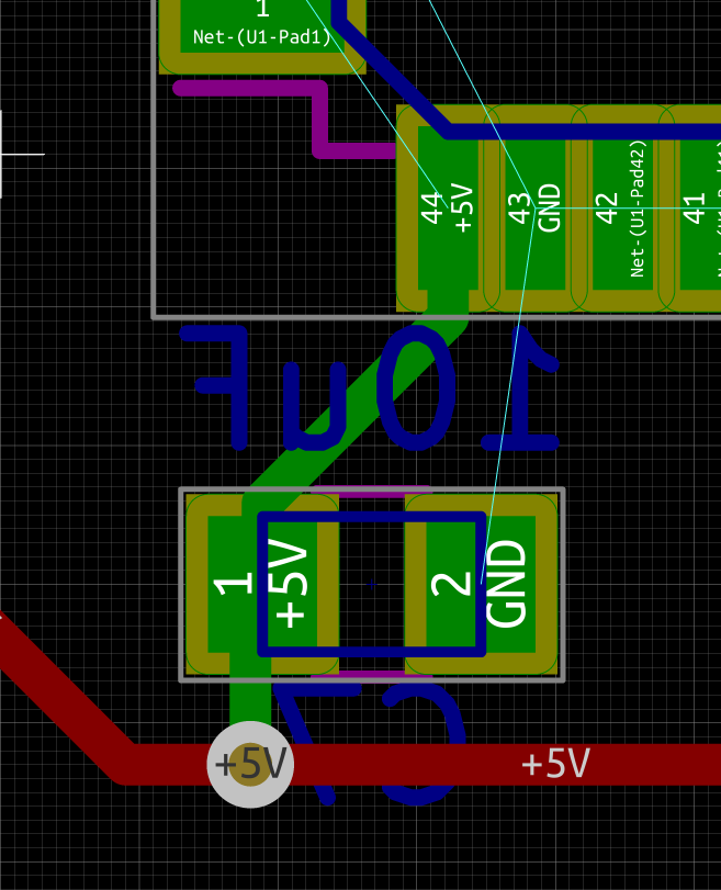
Do not route +5V through the inside of the MCU or change this order of link, or the decoupling capacitor will have very little effect.
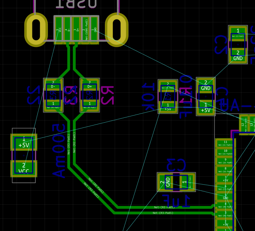
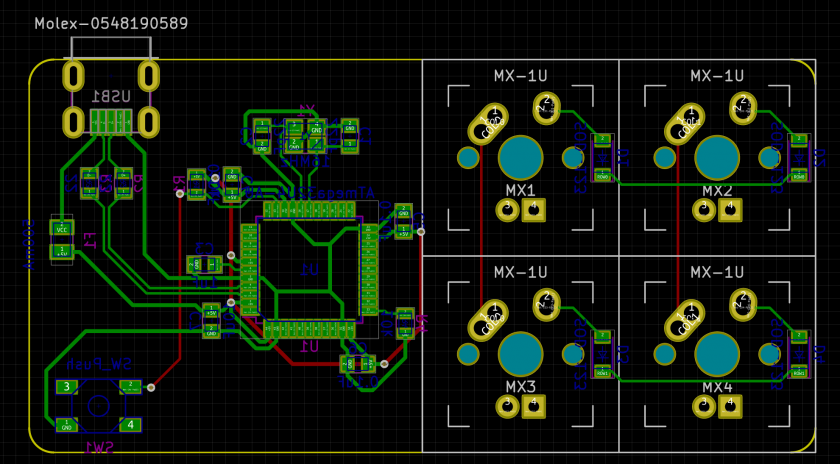
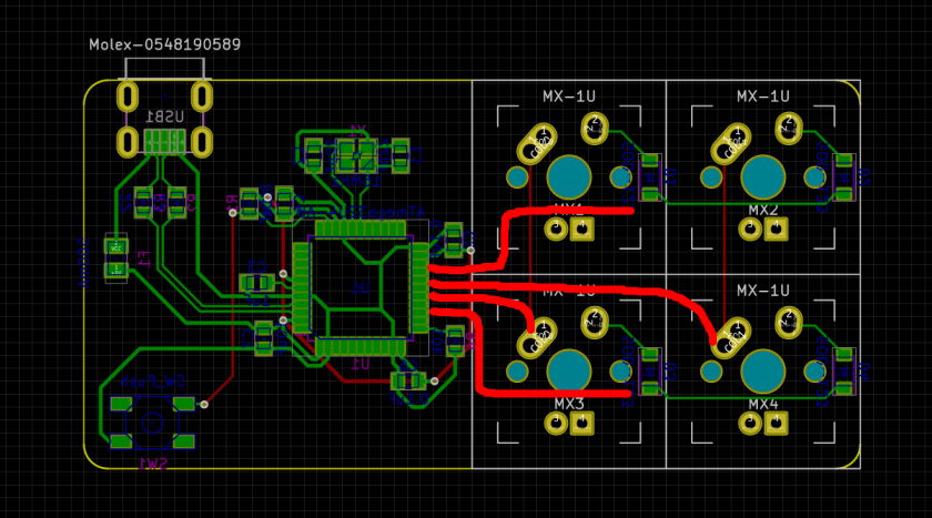
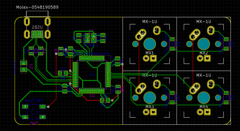
Here is a sample routed PCB.
After passing through the polyfuse, the +5V line passes through the 10uF capacitor, which acts as a general decoupler for the entire MCU. After passing through it, the +5V rail flips to the top of the PCB, where it draws a U to feed each VCC pin through its decoupling capacitor.
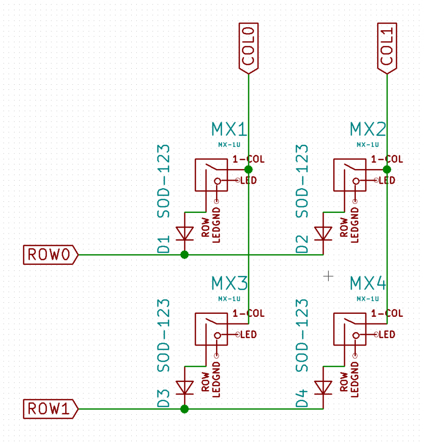
Step 10. Choosing the matrix pinout
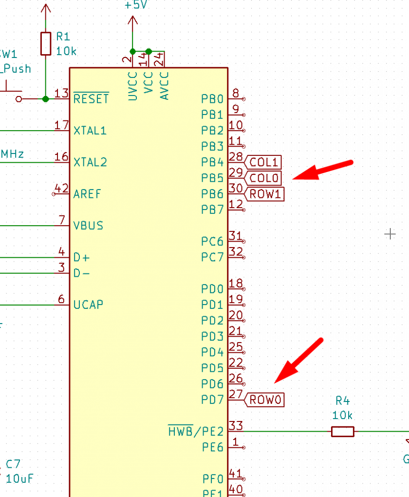
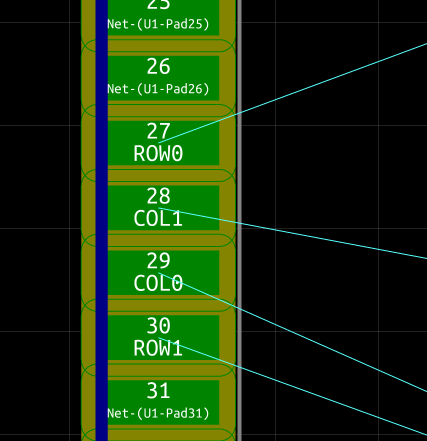
You may notice that the switches are not connected to the MCU at all.
This is because the pins to connect the matrix to are best chosen depending on the circumstance.
For example, it is much more logical to use these pins to the right,
Compared to attempting to desperately use the pins at the top left corner.
First, take a note of the pins you want to use,
and in the schematic editor, place the net labels for the rows and cols on the pins you wish to use.
Read these changes into the PCB.
The connections should appear on the MCU.
Quickly route these as well.
Congratulations! You have built your first keyboard PCB.
If you are not satisfied with the routing, you can go to Edit -> Global Deletions and check Tracks to restart.
Practice routing as many times as possible - It takes experience, not reading a tutorial, to learn the little tricks to route cleanly and efficiently.
Once you are finished, commit to GitHub. Then, it's time to add the final touch.